


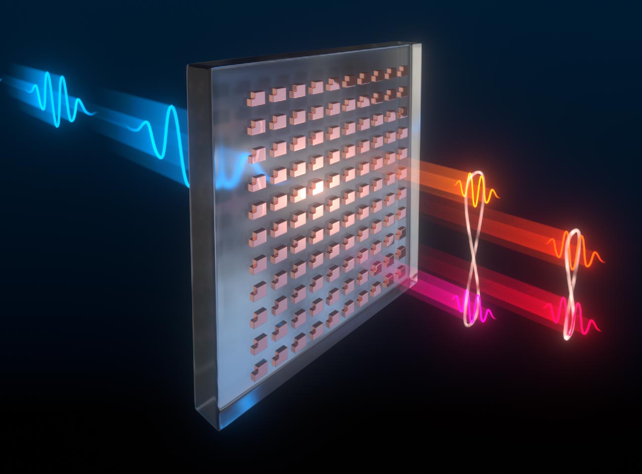
В представлении этого художника о сверхповерхности свет проходит через небольшие прямоугольные структуры — строительные блоки сверхповерхности — и создает пары запутанных фотонов с разными длинами волн. Устройство было разработано, изготовлено и испытано в рамках партнерства между Sandia National Laboratories и Институтом науки о свете Макса Планка. Фото: любезно предоставлено Игалом Бреннером, Sandia National Laboratories.
Сквозь количественное внешнее стекло
Помогая ученым контролировать странный, но полезный феномен квантовой механики, сверхтонкое изобретение может сделать будущие технологии вычислений, датчиков и кодирования заметно меньше и мощнее. Устройство описано в новом исследовании, опубликованном недавно в журнале наук.
По словам ученых из Национальной лаборатории Сандия и Института науки о свете Макса Планка, это устройство может заменить комнату, полную оборудования для связывания фотонов со странным квантовым эффектом, называемым запутанностью. Этот тип наноматериала, называемый суперповерхностью, прокладывает путь для фотонов, которые запутываются сложным образом, что было невозможно при использовании встроенных технологий.
Когда говорят, что фотоны запутаны, это означает, что они связаны таким образом, что действия влияют друг на друга, независимо от того, где и как далеко друг от друга находятся фотоны во Вселенной. Это пугающий эффект квантовой механики, законов физики, управляющих частицами и очень маленькими вещами.
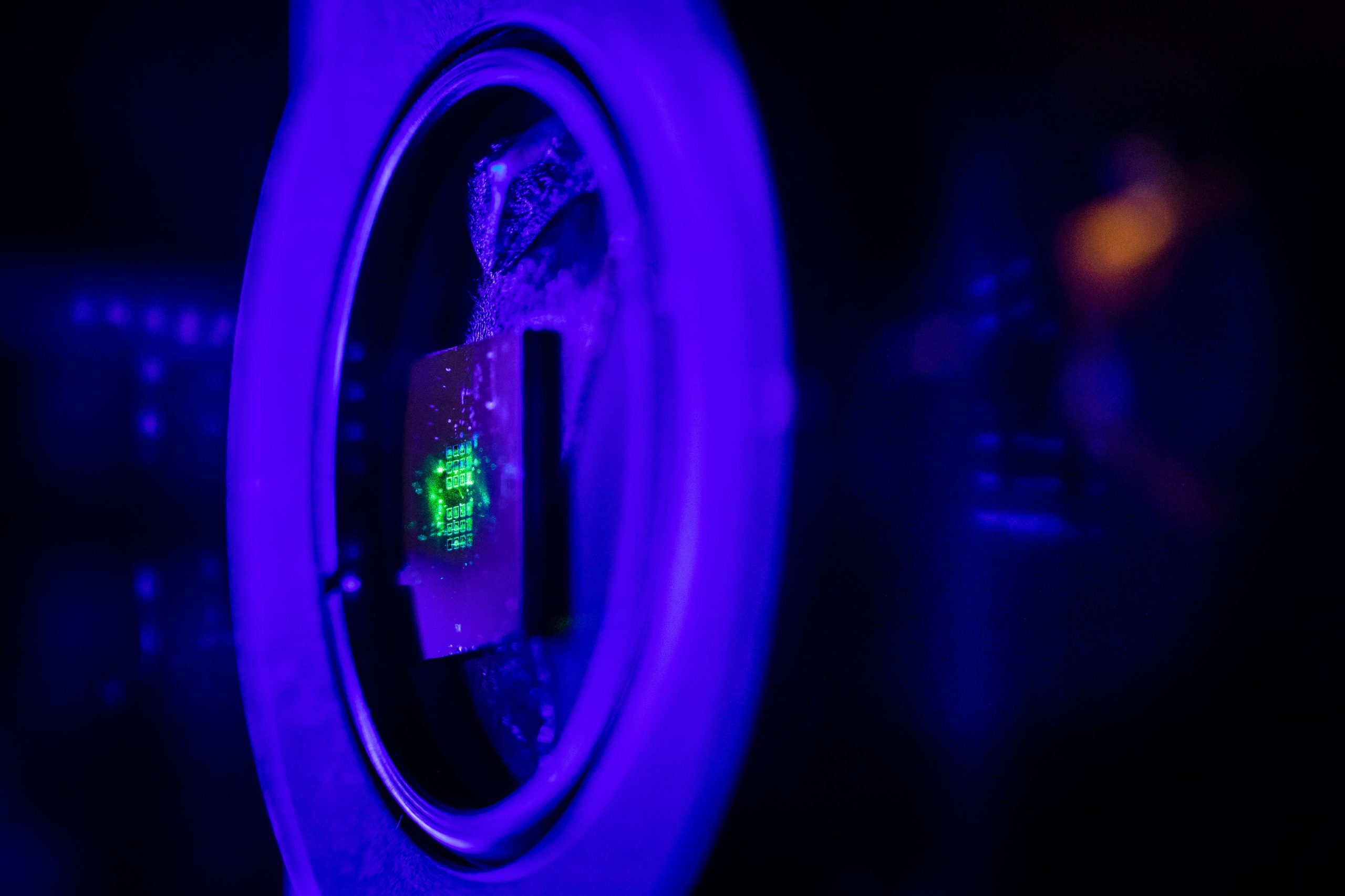
Зеленый свет лазера освещает поверхностную поверхность, которая в сто раз тоньше бумаги, изготовленной в Центре комплексных нанотехнологий. CINT совместно управляется Национальными лабораториями Сандия и Лос-Аламос Министерства энергетики, Управление науки. Авторы и права: Крейг Фриц, Sandia National Laboratories.
Хотя это явление может показаться странным, исследователи использовали его для обработки информации новыми способами. Например, запутанность помогает защитить точную количественную информацию и исправить ошибки в[{» attribute=»»>quantum computing, a field that may someday have sweeping impacts on science, finance, and national security. Entanglement is also enabling advanced new encryption methods for secure communication.
Research for the groundbreaking device, which is a hundred times thinner than a sheet of paper, was conducted, in part, at the Center for Integrated Nanotechnologies, a Department of Energy Office of Science user facility operated by Sandia and Los Alamos national laboratories. Sandia’s team received funding from the Office of Science, Basic Energy Sciences program.
Light goes in, entangled photons come out
The new metasurface acts as a portal to this unusual quantum phenomenon. In some ways, it’s like the mirror in Lewis Carroll’s “Through the Looking-Glass,” through which the young protagonist Alice experiences a strange, new world.
Instead of walking through their new device, scientists shine a laser through it. The beam of light passes through an ultrathin sample of glass covered in nanoscale structures made of a common semiconductor material called gallium arsenide.
“It scrambles all the optical fields,” said Sandia senior scientist Igal Brener. He is an expert in a field called nonlinear optics and led the Sandia team. Occasionally, he said, a pair of entangled photons at different wavelengths emerge from the sample in the same direction as the incoming laser beam.
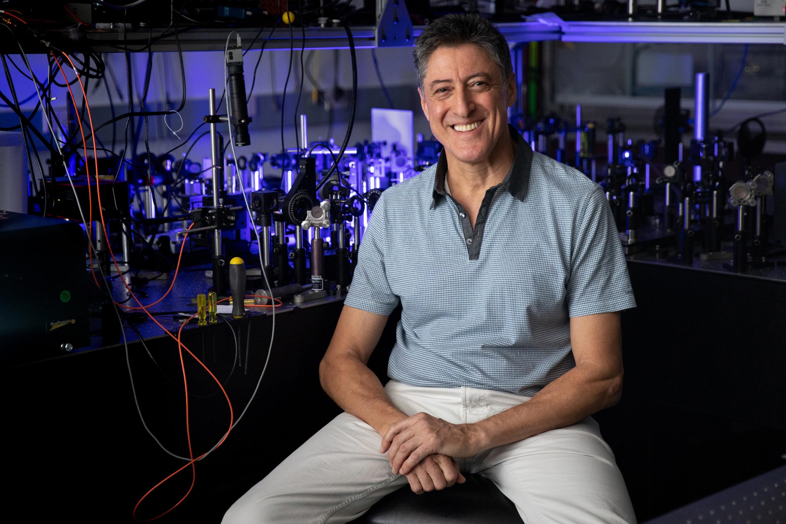
Sandia National Laboratories senior scientist Igal Brener, an expert in nonlinear optics, led a team that helped demonstrate a device that is paving the way for powerful, compact quantum information processing technologies. Credit: Craig Fritz, Sandia National Laboratories
Brener said he is enthusiastic about this device because it is designed to produce complex webs of entangled photons. Instead of just one pair at a time, it can produce several pairs all entangled together, and some that can be indistinguishable from each other. Some technologies require these complex varieties of so-called multi-entanglement for sophisticated information processing schemes.
Although other miniature technologies based on silicon photonics can also entangle photons, they lack the much-needed level of complex, multi-entanglement. Until now, the only way to produce such results was with multiple tables full of lasers, specialized crystals, and other optical equipment.
“It is quite complicated and kind of intractable when this multi-entanglement needs more than two or three pairs,” Brener said. “These nonlinear metasurfaces essentially achieve this task in one sample when before it would have required incredibly complex optical setups.”
The Science paper outlines how the team successfully tuned their metasurface to produce entangled photons with varying wavelengths. This was a critical precursor to generating several pairs of intricately entangled photons simultaneously.
However, the scientists note in their paper that the efficiency of their device — the rate at which they can generate groups of entangled photons — is lower than that of other techniques and will need to be improved.
What is a metasurface?
A metasurface is a synthetic material that interacts with light and other electromagnetic waves in ways conventional materials can’t. Brener said that commercial industries are busy developing metasurfaces because they take up less space and can do more with light than, for instance, a traditional lens.
“You now can replace lenses and thick optical elements with metasurfaces,” Brener said. “Those types of metasurfaces will revolutionize consumer products.”
Sandia is one of the leading institutions in the world performing research in metasurfaces and metamaterials. Between its Microsystems Engineering, Science and Applications complex, which manufactures compound semiconductors, and the nearby Center for Integrated Nanotechnologies, scientists have access to all the specialized tools they need to design, fabricate, and analyze these ambitious new materials.
“The work was challenging as it required precise nanofabrication technology to obtain the sharp, narrowband optical resonances that seed the quantum process of the work,” said Sylvain Gennaro, a former postdoctoral researcher at Sandia who worked on several aspects of the project.
The device was designed, fabricated, and tested through a partnership between Sandia and a research group led by physicist Maria Chekhova. She is an expert in the quantum entanglement of photons at the Max Planck Institute for the Science of Light.
“Metasurfaces are leading to a paradigm shift in quantum optics, combining ultrasmall sources of quantum light with far-reaching possibilities for quantum state engineering,” said Tomás Santiago-Cruz. He is a member of the Max Plank team and first author on the paper.
Brener, who has studied metamaterials for more than a decade, said this newest research could possibly spark a second revolution — one that sees these materials developed not just as a new kind of lens, but as a technology for quantum information processing and other new applications.
“There was one wave with metasurfaces that is already well established and on its way. Maybe there is a second wave of innovative applications coming,” he said.
Reference: “Resonant metasurfaces for generating complex quantum states” by Tomás Santiago-Cruz, Sylvain D. Gennaro, Oleg Mitrofanov, Sadhvikas Addamane, John Reno, Igal Brener and Maria V. Chekhova, 25 August 2022, Science.
DOI: 10.1126/science.abq8684

«Главный евангелист пива. Первопроходец в области кофе на протяжении всей жизни. Сертифицированный защитник Твиттера. Интернетоголик. Практикующий путешественник».
More Stories
Космическая компания стремится доставить жизненно важные грузы куда угодно в течение 90 минут.
Сообщество регби сплачивается за талантливого игрока после «разрушительного» диагноза.
Огромное доисторическое морское чудовище ростом выше двух автобусов было обнаружено после того, как 11-летняя британская девочка нашла окаменелости на пляже Сомерсет.